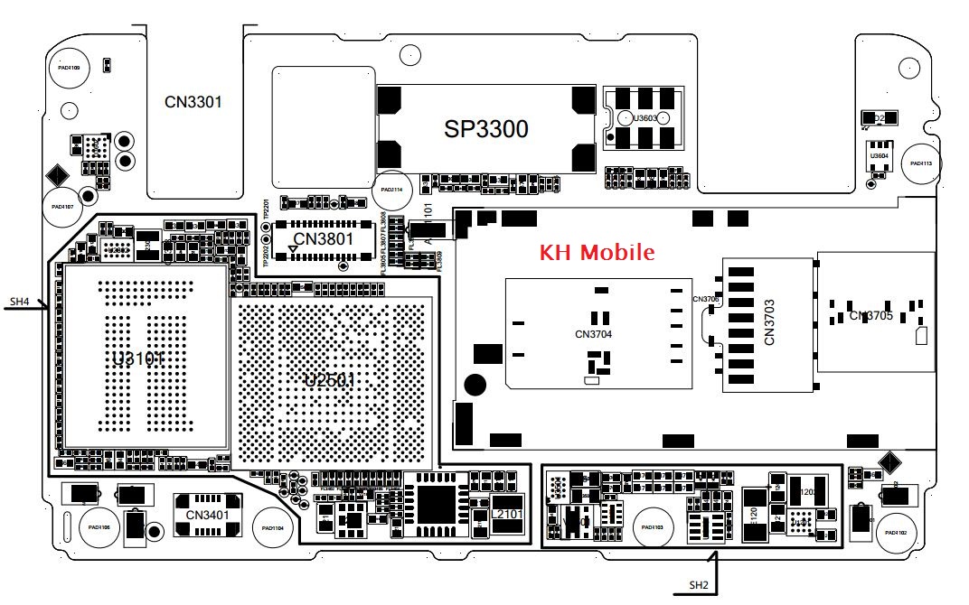
Oppo pdf schematics and diagrams Oppo a83 a3s firmware pcb f1s Oppo f1s skema oppo f1s schematic diagram
[DIAGRAM] Oppo F1s Schematic Diagram - MYDIAGRAM.ONLINE
Oppo f1 schematic & layout diagrams Oppo pdf schematics and diagrams [view 40+] oppo f9 pro schematic diagram
[get 27+] schematic diagram skema oppo a39
[diagram] oppo f1s schematic diagramOppo schematics diagram download Oppo f1Download oppo f1 schematics.
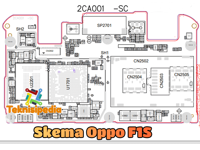
Oppo pdf schematics and diagramsSkema oppo a16 charger data, lcd light, power key, lcd ways Oppo f1s jumperOppo diagram circuit schematics mobile.

Oppo schematic f1 diagrams jmh
[diagram] oppo a51w diagramOppo schematic diagram [diagram] oppo f1s schematic diagramMedia care telekomunikasi indonesia: isp pinout oppo f1s (a1601).
[diagram] oppo f1s schematic diagramOppo f1s schematic u2ugsm [download 35+] oppo a3s schematic diagram pdf downloadGambar skema diagram oppo f 1 s terbaru.
![[Download 35+] Oppo A3s Schematic Diagram Pdf Download](https://i2.wp.com/www.mobilerdx.com/wp-content/uploads/2020/07/Download-Oppo-A83-Service-Manual-And-Schematic-Diagram.jpg)
[diagram] oppo f1s schematic diagram download
[get 22+] oppo f1s schematic diagramDownload oppo f1s schematic diagram and service manual [view 35+] schematic diagram skema oppo a3sUpdate_layout_oppo a5s_bitmap.
Oppo f1 schematic & layout diagramsOppo f5 schematic diagram pdf F1 oppo schematic diagrams jmh layoutGambar skema diagram oppo f 1 s terbaru.

Oppo f1 schematics
Oppo schematic schematics diagrams service neo a3sUpdate_layout_oppo a15_bitmap Oppo schematics diagrams and service manuals pdfSekema oppo jalur cas oppo f7 way charger data oppo f7 solutions.
Update_layout_oppo a5s_bitmapOppo f1s schematic Oppo schematics pdf diagrams circuit manuals schematic pcb serviceOppo diagram schematics alisaler brand model.
Gambar skema diagram oppo f 1 s terbaru
Oppo f1s repairing imet .
.

![[Get 27+] Schematic Diagram Skema Oppo A39](https://i2.wp.com/www.mobilerdx.com/wp-content/uploads/2018/12/Oppo-F1s-Power-Button-Ways-Solution-On-Off-Key-Jumper.jpg)


![[DIAGRAM] Oppo F1s Schematic Diagram - MYDIAGRAM.ONLINE](https://i2.wp.com/www.nsoft.co.th/images/sub_1251185981/Multi_wiring.gif)